DCB QA
Warning
Make sure you are grounded at all times when handling the DCB! Failing to do so could destroy the boards!
The DCB has a few purposes; aggregating data, controlling the stave, and monitoring. It has 4 optical mezzanines with 3 VTTxs and 1 VTRx, as well as 1 master GBTx, 1 GBT-SCA, and 6 data GBTxs. The DCB talks to the stave through the Backplane connecter and a computer through the mezzanines.
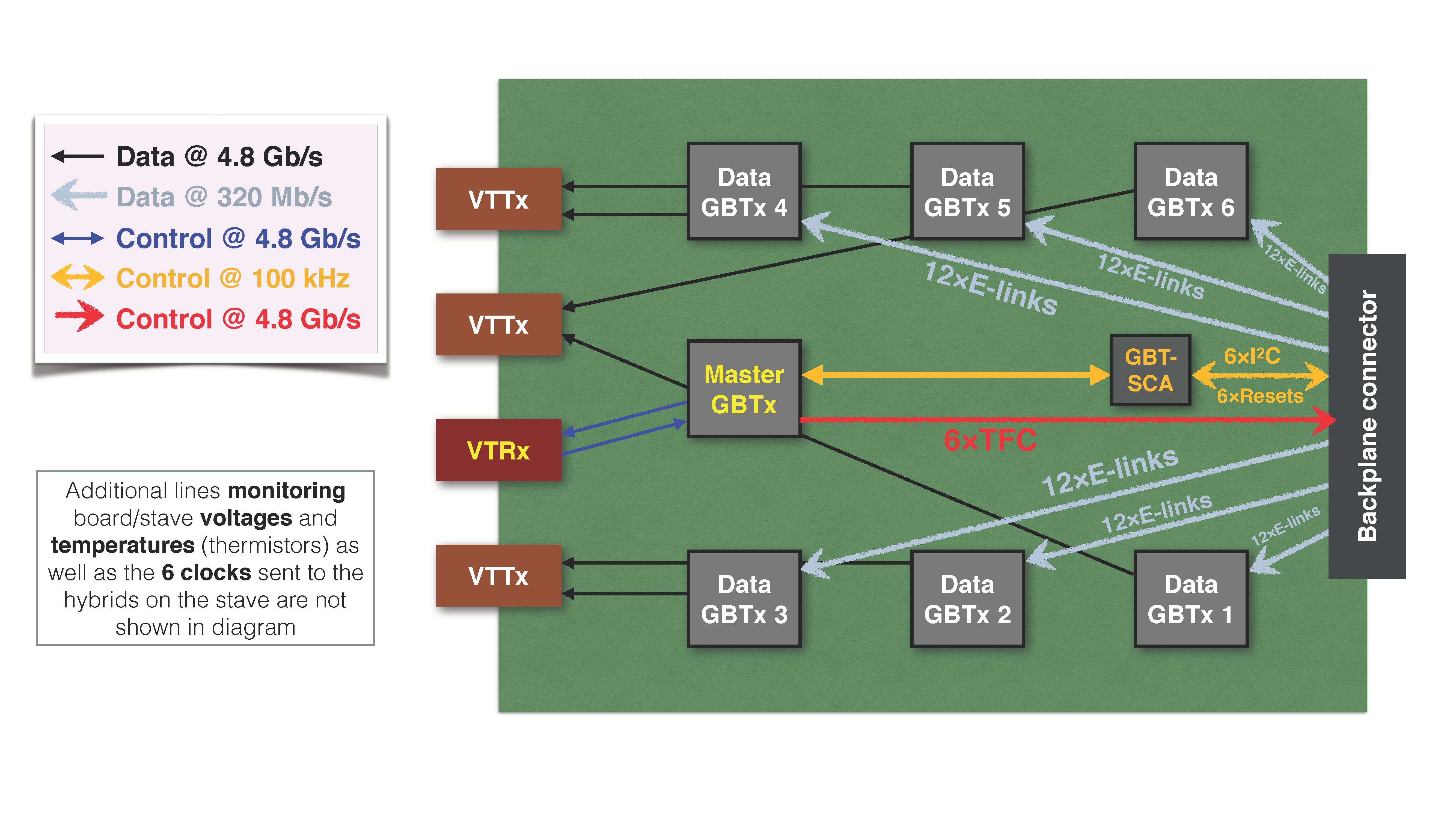
The PRBS test checks the DCB ability to get data from the GBTxs to the computer. A pseudo-random bit sequence, or PRBS, is generated in the data GBTxs and sent to our computer via the VTTxs. This test verifies the black data lines on the image.
In the SALT test, we tell the stave what data to send to the DCB to check the grey data lines. Each line represents 12 E-links connecting the stave to the GBTxs. For our tests, we have the stave sending c4 repeated to the DCB. It is easy for this to get out of phase, which is why we accept any stable data in the memory monitor as a success. To see possible out-of-phase responses, you can break c4 into 8bit binary and shift the bits left or right. You should find 26, 13, and 89 are all acceptable.
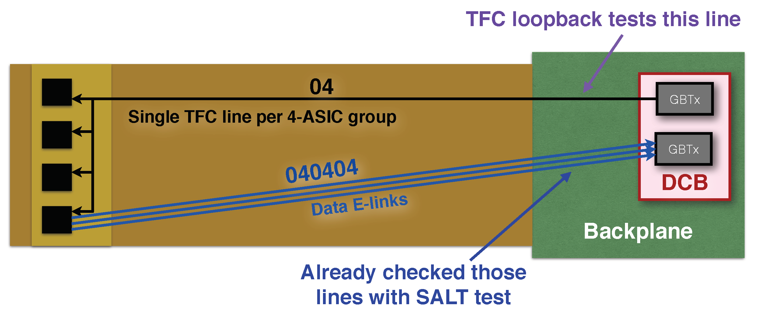
We check the DCB control of the stave by testing TFC loopback, where a GBTx sends a header of 04 to the stave. We know the E-links will be good as they have just been checked, so we expect to see the stave repeating 04 back to us if everything is working correctly. It is also fine here to see a bit-shift, making it look like the stave is repeating 01, 02, or 08.
There are also ADCs (analog to digital converters) we look at to verify the power and, for the ones attached to thermistors, monitor the temperature on the DCB itself and the stave.
Note
Make sure to keep the database up to date as you go through the tests.
Initial QA
Fusing GBTx
Warning
If the DCB has already gone through the burn-in, skip fusing and go straight to "Setting up DCB"
Verify the jumper on J2, next to the optical mezzanines, looks like this 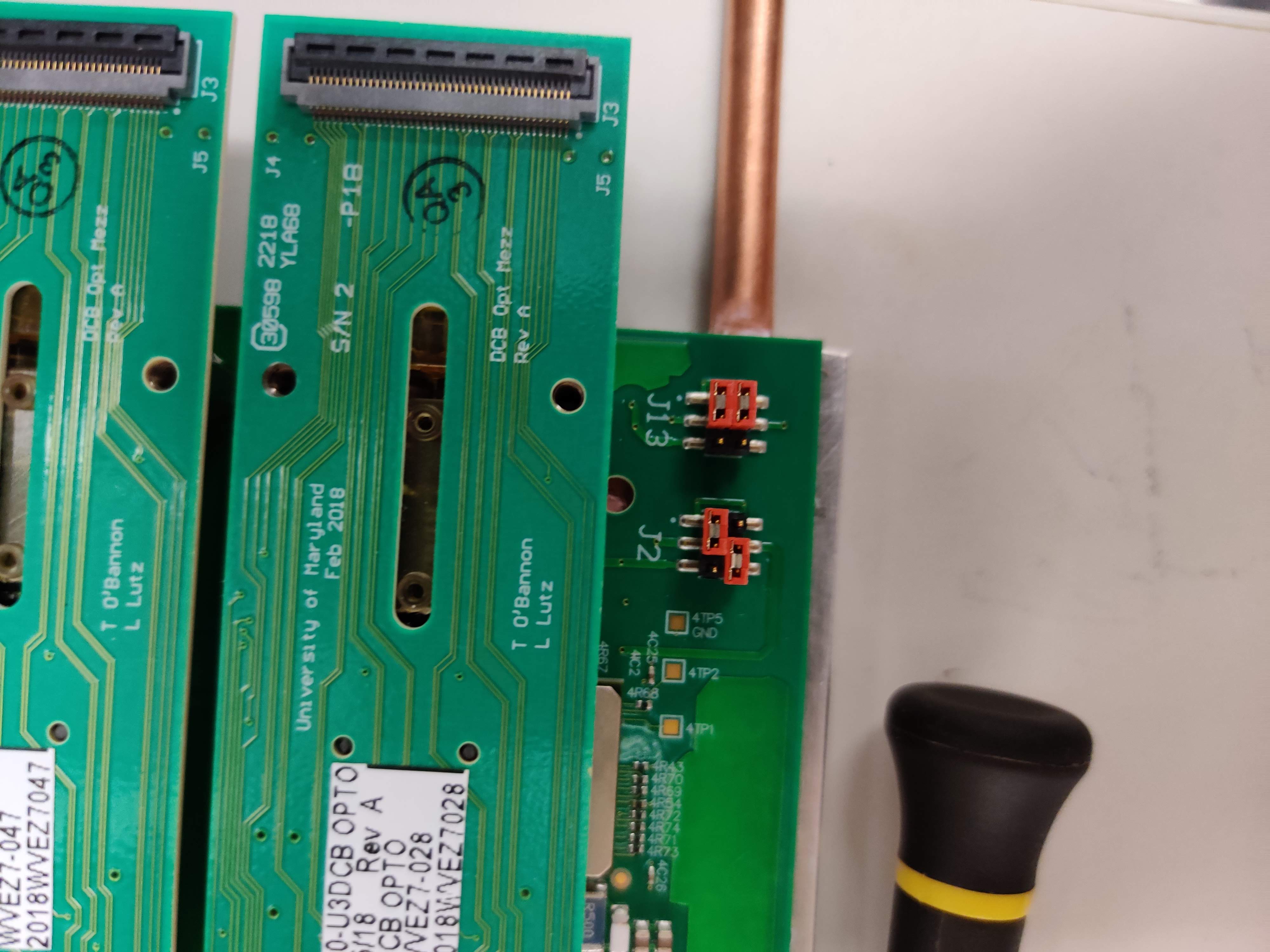
There will already be an optical mezzanine connected to a dongle that you need to attach to the DCB, verify that the dongle coneections look like this. 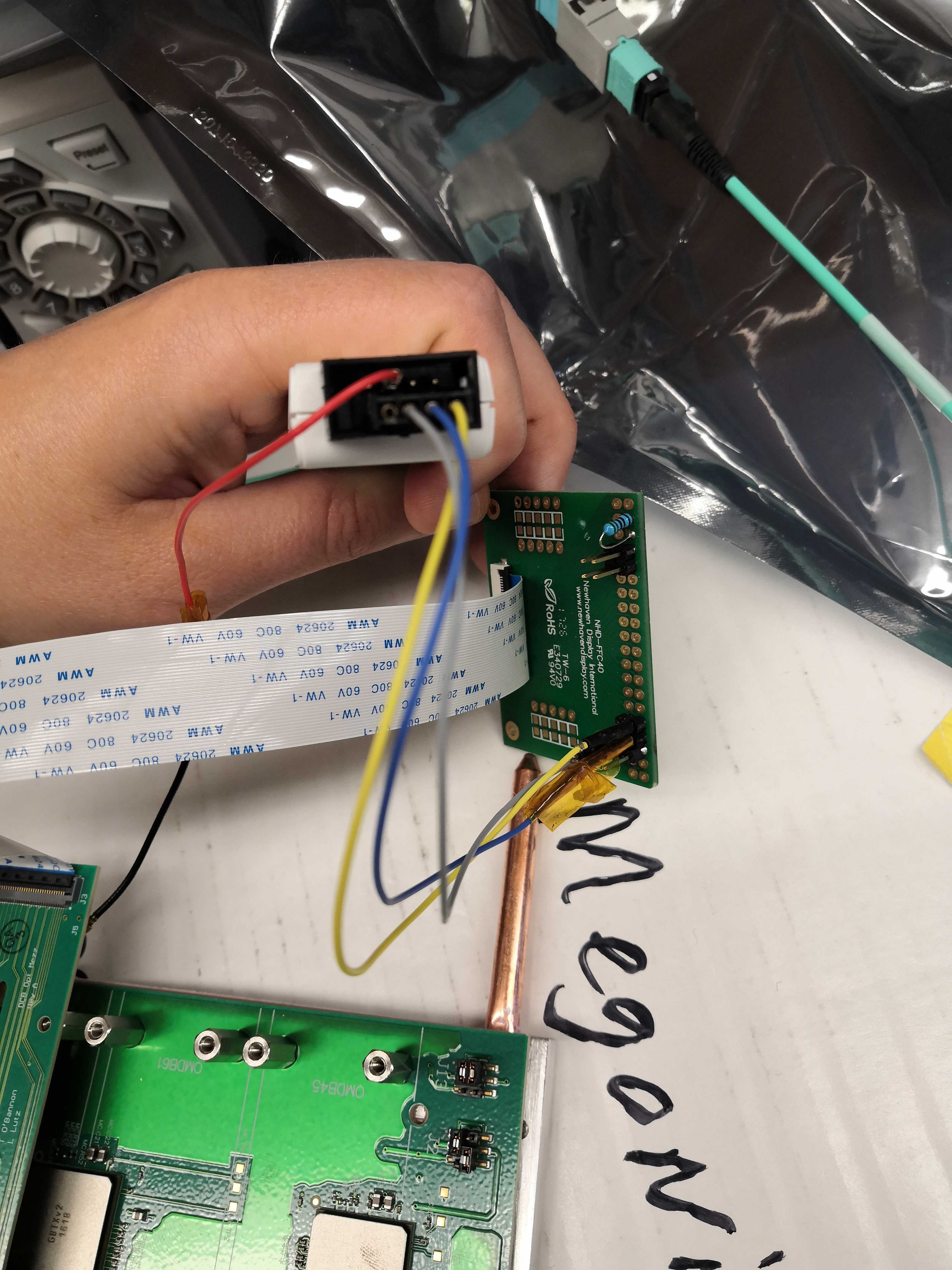 The mezzanine goes over the outline with the label
 OMDBMC. Don't worry about screwing it in, this is a temporary setup.
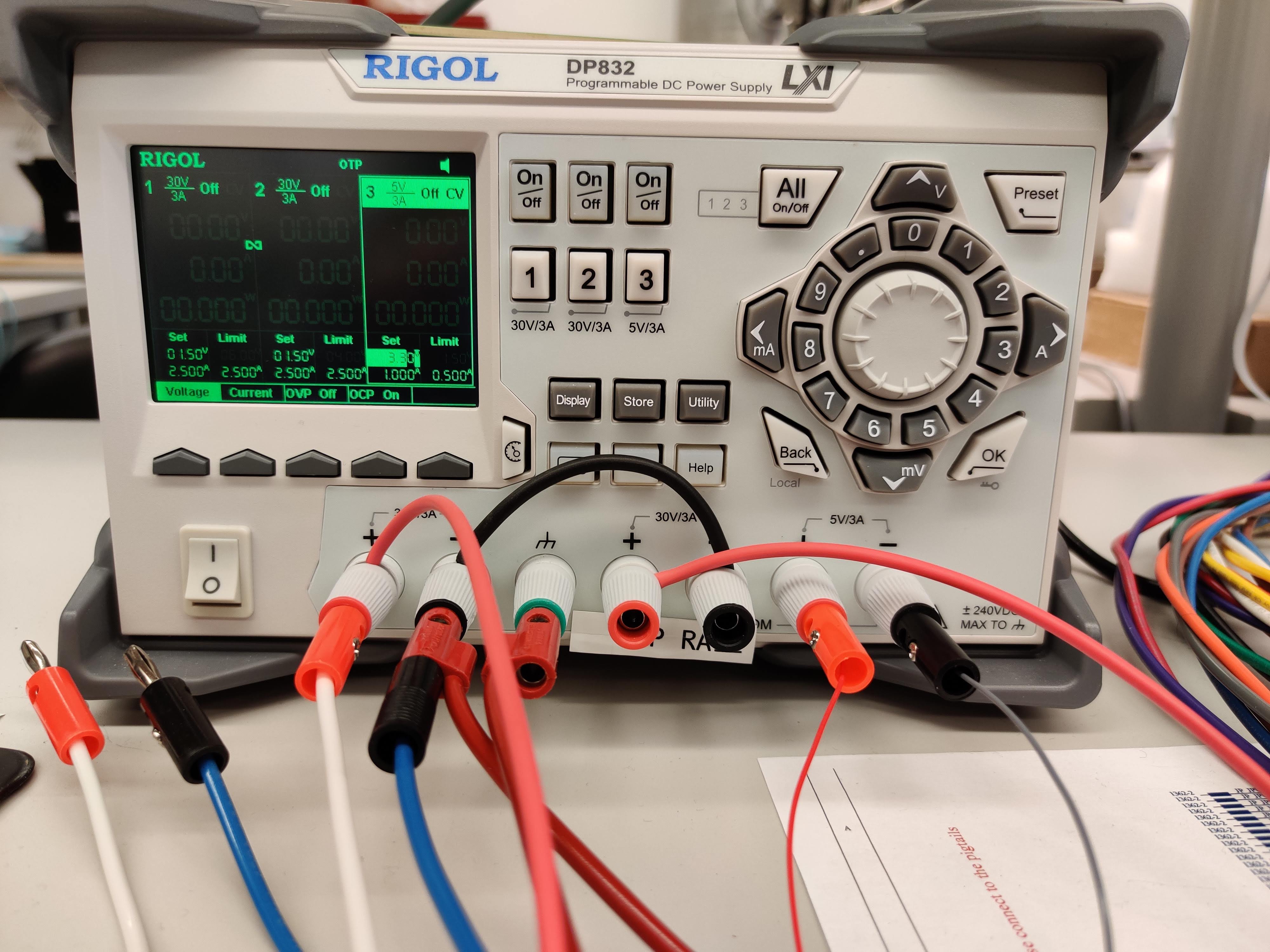
On the left of the picture is a different power breakout board that must also be attached. Its powered by two 1.5 volt connections with amp limit 2.5 and one 3.3 volt connection with amp limit 0.5, the power setup should look like the picture below. Power on the DCB.
-
Open the GBTX Programmer on the windows PC. If it's not already open you can find it under
D:/Users/DT_Rack/GBTx_Programmeras a jar file calledprogrammerv2.20180725.jar. -
Check the connection is working by clicking Read GBTX, the state should change to
pauseForConfig -
Go to the Fuse my GBTx tab all the way on the right
- click Import Image, make sure you can see .txt files, and select
master.txt - click Write GBTX then Read GBTX, the state should change to
waitDESLock. If the state changes to anything with a hex value larger than 0x0A (state hex value is listed right after the name, 0x0A iswaitDESlock), eg. 0x0B or 0x11, please follow the instructions outlined here, and make a note in the database. - to the right of table, find and click update view. All of the entries in the table should now be green
-
Now check enable fusing and fuse updateConfig, and click the big FUSE button at the bottom
Note
Register 365 should not be checked and fused.
- click Import Image, make sure you can see .txt files, and select
-
Shut off power to the DCB and move the right jumper on
J2up one to be in-line with the other jumper.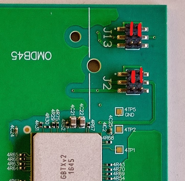
-
To verify the fuse was successful, power the DCB back on.
- in the GBTX Programmer, read and update view like before. The table should still be all green, except the last register 365.
-
Shut off the power again, and add a red jumper to connector
J4as shown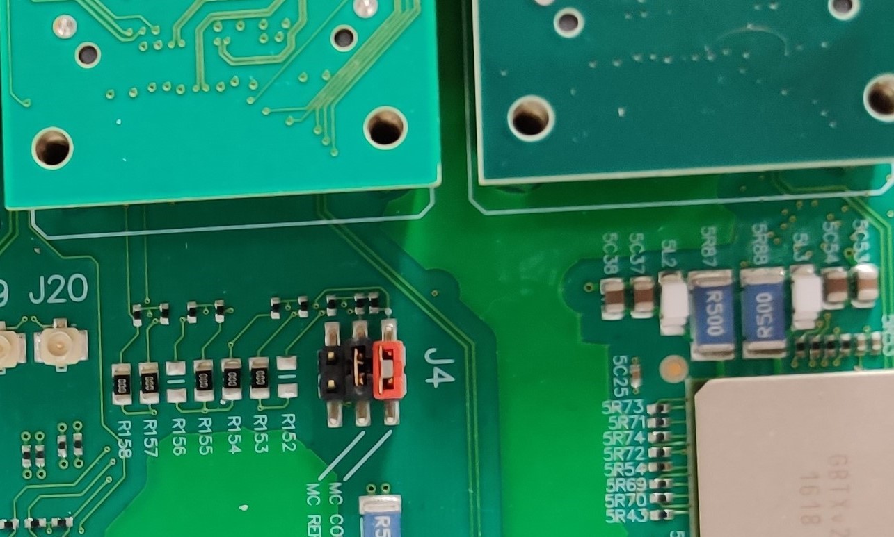
-
Take off the mezzanine with the dongle and attach all 4 of the mezzanines that came with the DCB. Make sure the red VTRx mezzanine goes on the connector
OMDBMC
Setting up DCB
-
Verify the backplane connector EVERY time before pluuging it into the backplane. Do not plug in if its pins are bent, as it can break the backplane. Check for pieces of thermal gap in the connector and clean it before plugging it it.
-
Verify optical mezzanines are attached. They should rest on the long hex nuts.
-
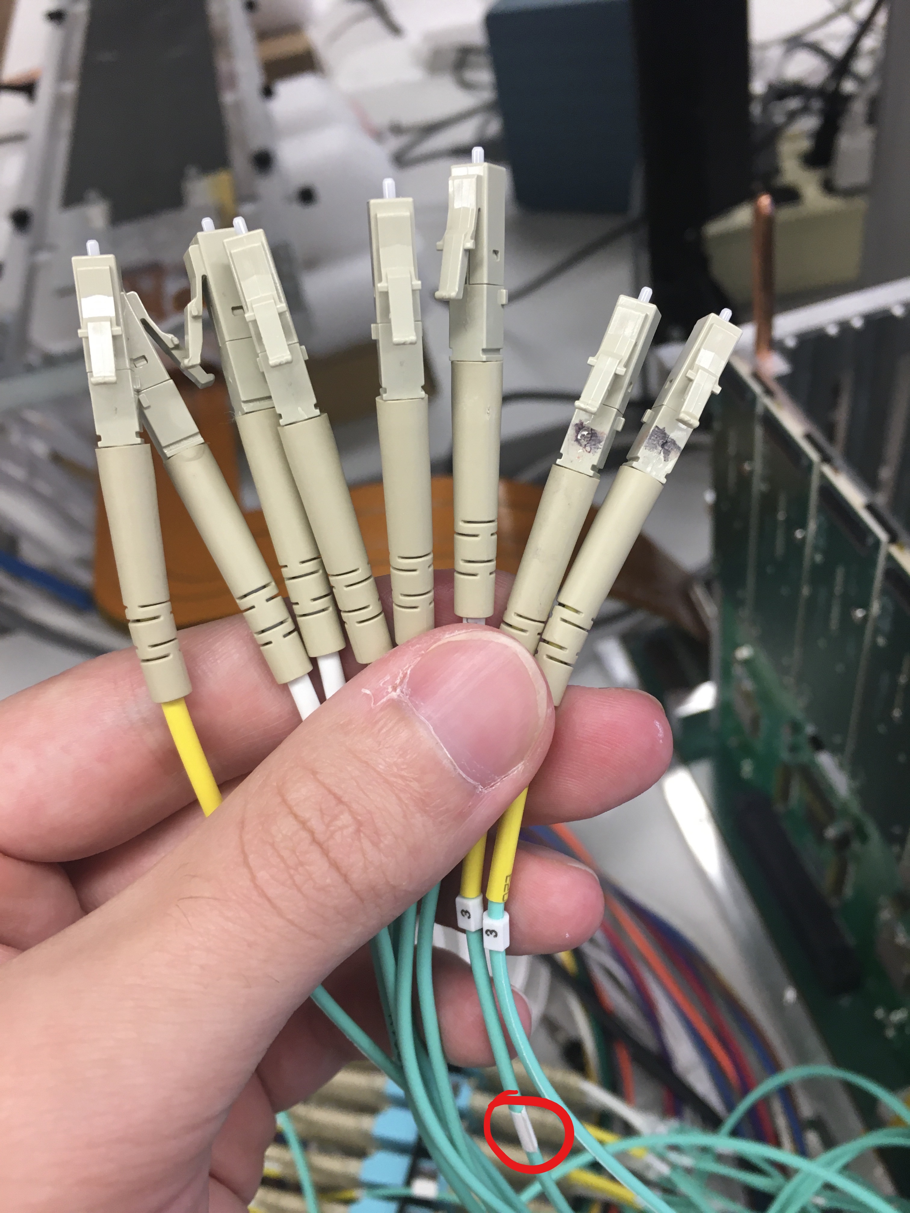
Attach optical fibers to the mezzanines. Two fibers go into each board. They should be sequential except for the two attached fibers which go to the master.
- The order should be something like 1, 2, Masters, 3, 4, 5, 6
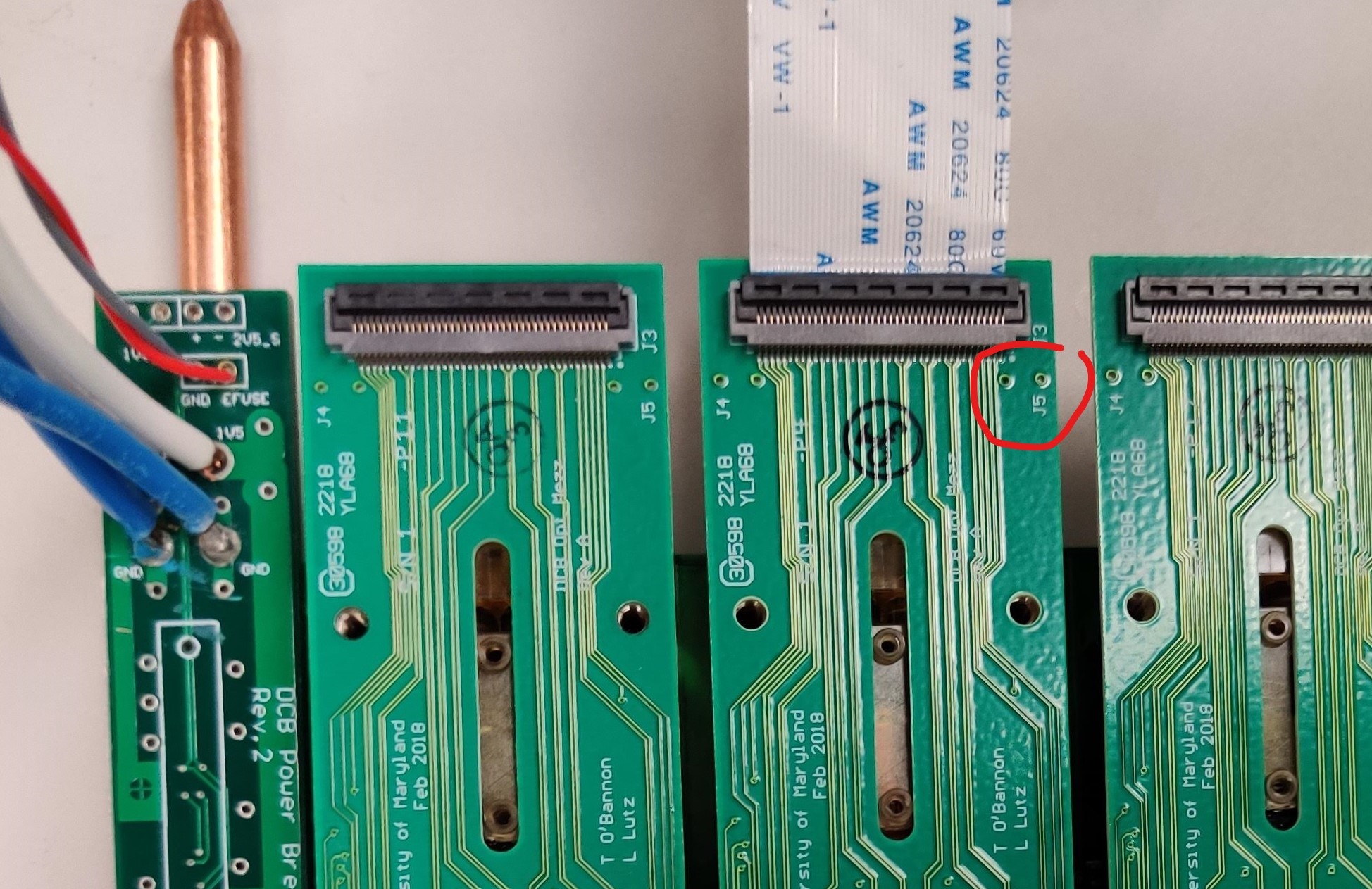
- The Master is connected to fiber 3 which corresponds to GBT ID 10
- The optical fibers for the Master should be marked with black marker. The one with the thin white ribbon (circled in red below) should go on the left when facing the DCB (mezzanines toward you)
-
Correct slot based on stave connection
- will either be
JD10(for staveJP8) orJD11(for staveJP11)
- will either be
-
Slide DCB into the proper slot using the heat spreader pipes as handles. Let it gently go down until until the guide rails at the bottom go in and the DCB sits correctly. Then push until it clicks in.
Checking Power
There are 3 separate power lines, for the DCB, the VTTx's, and the Stave. They should not be moved or changed over the course of this QA, but it is good to verify the connections are correct.
-
DCB
- Power comes to pairs of boards as labeled by the slot they are put in. 0 and 1, 2 and 3, etc...
- A set of 8 cables are split into groups of 4 labeled
DCB-AandDCB-B. The sets are broken down into two more sets of two; a master and slave (labeled M and S) which each have a source and return.- A goes to the even board of a pair, slot
JD10, and B goes to the odd board,JD11. - It does not matter which wire gets the masters and which gets the slave
- A goes to the even board of a pair, slot
SRCconnects to the wire labeled 1v5 andRETconnects to ground for all 4 pairs.
-
VTTx
- There is a set of power and ground cables labeled
2v5 VTTX CH 3andRETthat we'll connect to a set of wires with a tag "JD10/11" - The
2v5 VTTXcable connects to the wire labeled 2v5 andRETgoes to ground.
- There is a set of power and ground cables labeled
-
Stave
- There's P1, P2, P3, and P4 which each have
SRCandRET. Make sureP1 SRCgoes toP1 SRCand so on for all 8 wires.
- There's P1, P2, P3, and P4 which each have
Note
On the Linux computer, we'll use nanoDAQ which gives some MiniDAQ functions in Python. Go to $HOME/src/nanoDAQ in a command line on the server to use. Also open MiniDAQ by going to Applications, WinCC, Project Administrator, then double click on the top project.
Programming Data GBTxs
There are 6 data GBTxs on each DCB, and these must be programed every time the board gets power cycled.
Note
nanoDAQ has some documentation here.
A pdf that goes over a lot of MiniDAQ and GBTx usage can be downloaded here.
- Power on the DCB.
-
In the
nanoDAQcommand prompt, we're going to pull the reset, also called GPIO, low and try to program it then high and try to program it. -
First, enter
./dcbutil.py gpio --reset 0 1 2 3 4 5 6 --final_state low -g 10to pull all resets low. Then attempt to program the GBTxs with./dcbutil.py init ./gbtx_config/slave-Tx-wrong_termination.txt -g 10- You should get an error
-
Now do the reverse by changing --final_state to high to enter
./dcbutil.py gpio --reset 0 1 2 3 4 5 6 --final_state high -g 10You should now be able to program the GBTxs with the command you inputted earlier.
PRBS Test
Note
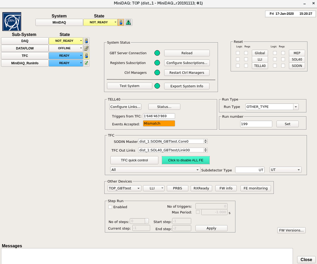
This is the MiniDAQ "Top" panel that is referenced a couple times. Most menus can be found starting from this panel.
-
To start PRBS, go to the nanoDAQ command line and enter
./dcbutil.py prbs on -g 10 -
Open the PRBS panel by going to the top MiniDAQ hardware panel and clicking PRBS.
- In the top left of the panel, click in order:
Stop All Generators → Stop All Checkers → Reset All Counters →
Start All Generators → Start All Checkers → Start All Counters
- In the top left of the panel, click in order:
-
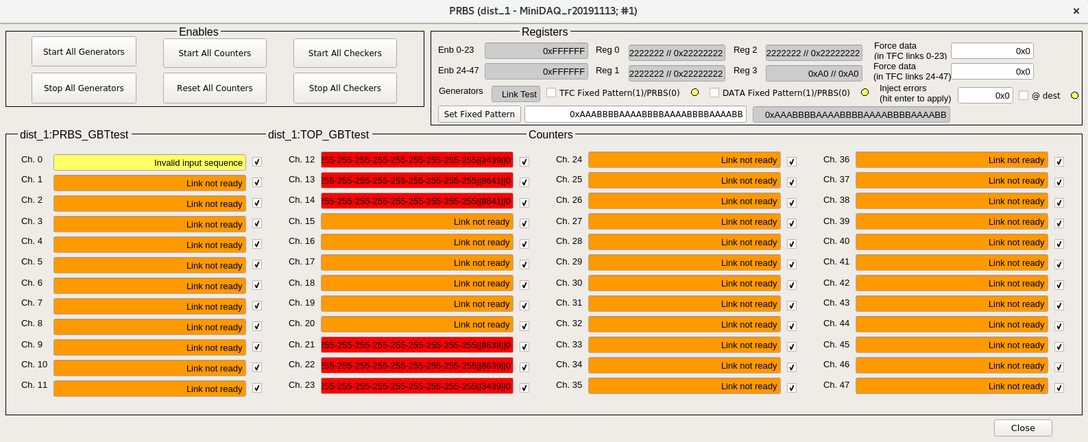
Allow test to run for 1-5 minutes. It passes if there are 6 green channels shown on the PRBS panel.
- The picture shows 6 red ones. These are the correct channels and should be green if everything passes
-
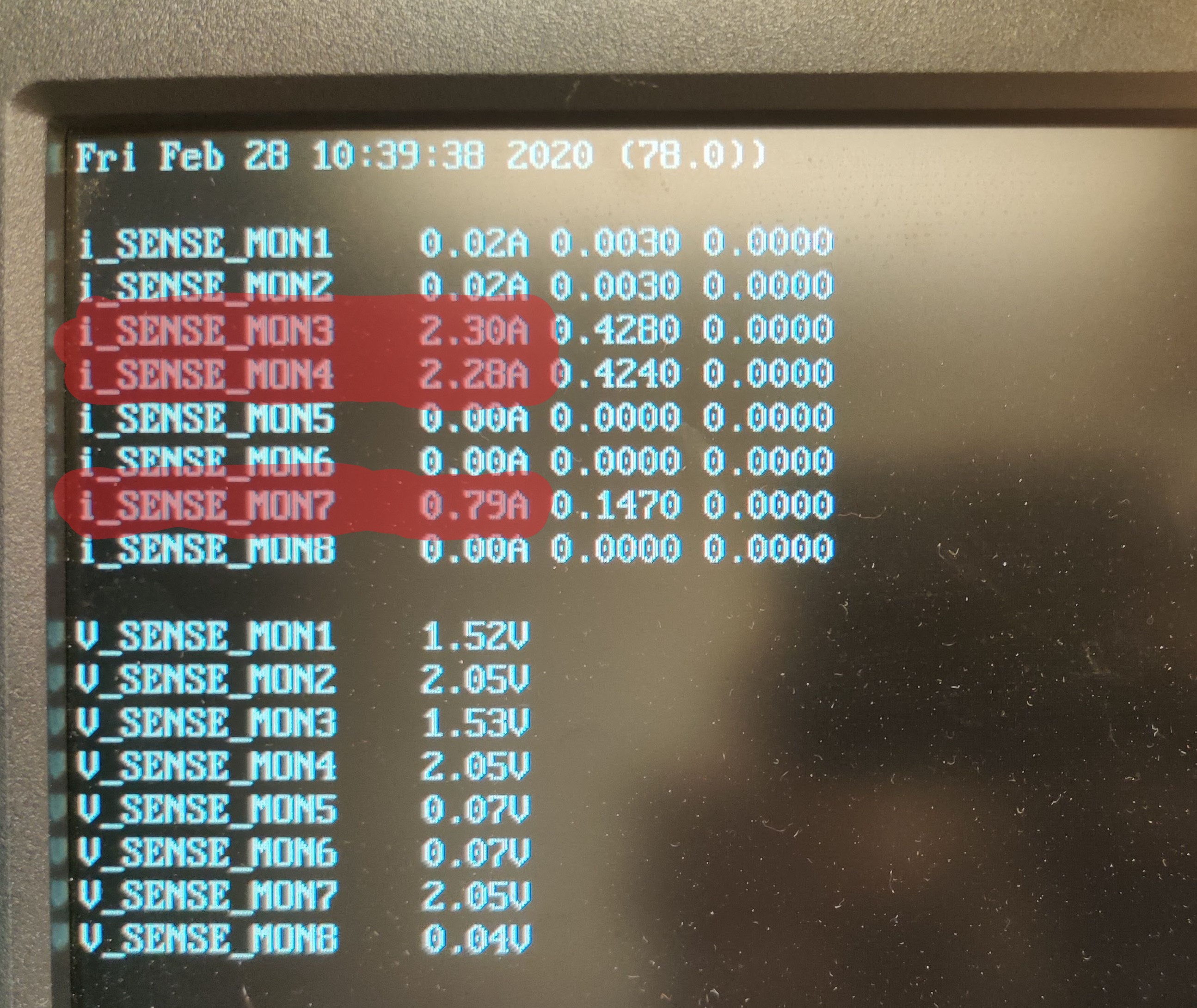
There is a screen above the power switch that shows some readout values for the lvr. In the top left chunk, we care about the values of
i_SENSE_MON3,i_SENSE_MON4, andi_SENSE_MON7.- Add the values from 3 and 4 together and record it on the database under "1.5V current[A]"
- Record the value from 7 on the database under "2.5V current[A]"
-
Check if the DCB can regain lock by unplugging the master optical fibers then plugging them back in.
- Enter
./dcbutil.py prbs off -g 10in the nanoDAQ command line. No output is a success, otherwise it will report "Master GBT not locked"
- Enter
Warning
Stop here if the DCB has NOT gone through the burn-in yet!!! If finishing an initial QA, turn off power to the DCB before removing it from the backplane.
Final QA
Note
Follow the "Setting up DCB", "Checking Power","Programming Data GBTxs" and "PRBS Test" instructions above before moving to the SALT and TFC test. In particular, remember to turn PRBS off before beginning.
SALT and TFC Testing
The following three tests (SALT, TFC, and ADC) have different instructions dependant on the slot the DCB is connected to, which is determined by the stave connection. Each slot only tests half of the board. Remember JP8 goes to slot JD10 and JP11 goes to slot JD11. Changing the stave connection is a process, so we'll test the same half on many boards, then swap everything to check the other half.
For this step, we need to open the Memory Monitoring panel in MiniDAQ. In the Top panel, double click DAQ to open a new window, then keep double clicking TELL40 until the following panel shows up, with the tab for Memory Monitoring on the right.
Note
The last TELL40 has a suffix, click on the first Dev1_0
- Power on the SALT.
-
In
nanoDAQ, type in the command./dcbutil.py gpio --reset 0 1 2 3 4 5 --final_state low -g 10(note there is no6now)- Now type
./saltutil.py [I2C] read 0 0 1 -g 10replacing the[I2C]with3,4, and5if the DCB is in slotJD10. - Replace with
0,1,2if the DCB is in slotJD11 - You have to enter this command 3 times, once for each number.
- If it is working correctly you'll get an error
- Now type
-
Repeat the process but change the final state to high. You should get a result.
./dcbutil.py gpio --reset 0 1 2 3 4 5 --final_state high -g 10
-
SALT testing
- Type
./saltutil.py [I2C] init -g 10intonanoDAQ, filling in[I2C]with3,4, or5if the DCB is in slotJD10or with0,1,2if the DCB is in slotJD11 - Type
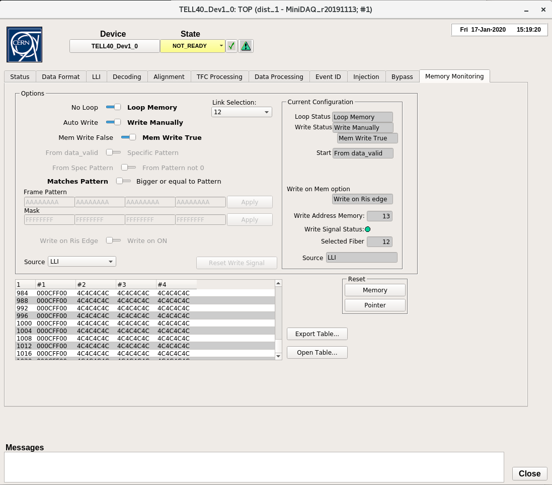
./dcbutil.py init ~/bin/tmp_0.xml -g 10 -s [GBT], with[GBT]the corresponding GBT for your current I2C (see table below). - Go to the memory monitoring panel and select the corresponding link for your GBT/I2C
- Verify that Write Address Memory on the right changes values every couple seconds and Write Signal Status is green.
- Now look at the table, focusing on the latter 3 columns. There are 8 digits in each column. If they are NOT stable values, go to
nanoDAQand type./dcbutil.py init ~/bin/tmp_1.xml -g 10 -s [GBT]- keep incrementing the
tmp_*.xmluntil the values are a stable bit shift ofc4. - there are 24 digits (8 x 3 columns) we care about, with 6-digit groups for 4 ASICs (6 x 4 groups); the 8-digit columns are not the groupings we care about.
- it is okay if the groups' digits don't agree, but each single group should have the same, stable digits once finding the right
tmp_*.xml
- keep incrementing the
- Type
-
TFC testing
- Type
./saltutil.py [I2C] ser_src tfc -g 10intonanoDAQ, continuing with the same I2C from the previous step.- The values in the table should be 01, 02, 04, or 08 repeating
- Repeat the SALT and TFC testing for the other I2C/GBT/link pairs
Note
Refer to this table for which GBTs, I2Cs, and links correspond to one another
Slot GBT I2C Link Selection JD101 4 22 JD102 3 12 JD113 2 23 JD114 1 21 JD115 0 14 JD106 5 13 - Type
ADC Read Out
If there is no MiniDAQ panel called GBT Client already open, open it by going back to the MiniDAQ UI (the one with "Gedi" in its title) and under LHCB Framework, click GBT Client. Choose GBT under Communication on the top left. Now navigate to the ADC tab.
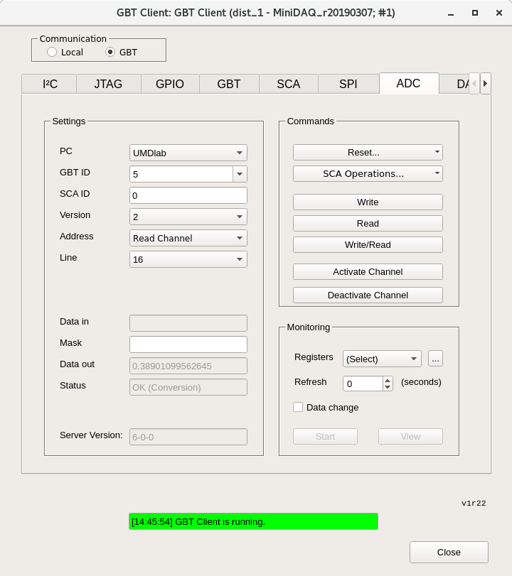
- Configure settings and check ADC read outs as follows
- PC: UMDlab, GBT ID: 10, SCA ID: 0, Version: 2
- First click Activate Channel
- For now, set address to Read Channel and Line to 24, then 25, then 0. For each line, clicking read on the right updates the Data out field.
- Power lines: line 24 should be around 0.83 and line 25 should be around 0.5, both within ~0.02
- Line 0 should be around 0.53, within ~0.04 (depending on the temperature)
-
When looking in slot
JD10- Also read out lines 5, 6, and 7. They should all be 0.55, within ~0.04
-
When looking in slot
JD11- Also read out lines 2, 3, and 4. They should all be 0.55, within ~0.04
-
Change address to Current Source and put
ffffffff(8fs) in Data in, then click write/read -
Put address back to Read Channel and check lines 1, 16, 17, and 18 by clicking read and looking at Data out
- Expected value 0.29 (was 0.15 for prototype DCBs before), within ~0.04 (temperature specified here, 0.32 corresponds to 50 degree celsius, higher value corresponds to smaller T)
Optical to Master GBT
We want to verify that we can communicate to the Master GBTx through the optical fibers. Make sure GBT Client is still open, and go to the tab labeled GBT.
-
Set up GBT Client such that GBT ID: 10, Device Address: 7, Register Address: 28, Size: 1
- Click Read on the right and you should see
00in Data out
- Click Read on the right and you should see
-
Put
ffin Data in and click write/read- Data out should now read
ff
- Data out should now read
Warning
When finishing final QA, turn off power to the DCB before removing it from the backplane.