LVR Setup/Initial QA
If you are already familiar with this procedure, you can simply follow the LVR initial QA checklist.
Before you proceed
-
Beware that
TP5is NOT GND. The silkscreen label applies to the adjacentTP2. -
Caution is needed when connecting test lead clips to the test points. The test points are rather fragile and easily pulled of the board.
-
Care must be taken to avoid temporary unintended shorts from the high density of surrounding components, vias, and traces.
-
Visually inspect a new LVR and set the switches as indicated in the table below. Order refers to toggles 1234 on the switch, with
1meaningON. (CCM) or (FPGA) refer to the side of the LVR the switch is on. There are four SW6 switches.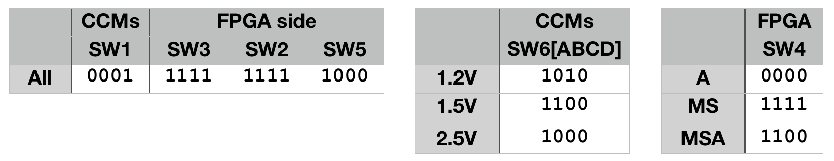
-
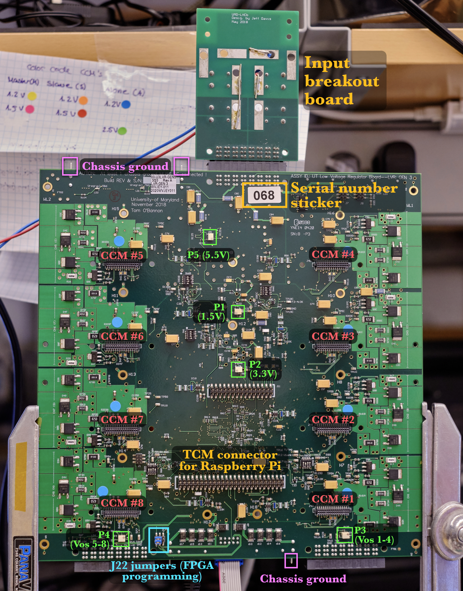
Place the LVR on the holder as shown in the picture. The CCM side should be facing you and the input connector be at the top. Recall that the one input is on one end and the two outputs on the other.
-
Place an serial number sticker on a new LVR under the input connector, and document its serial number in the database. Also document which type of LVR you intend to QA (12MS, 12A, 12MSA, 15MS, 25A).
- You don't need to fill every column in the database as you complete that test until you finish the QA or leave the setup for any reason.
- The CCM serial number is documented at a later stage, during LVR assembly.
-
Verify that the chassis and power ground are isolated by > 25k Ohms (often 180k Ohms)
- Measure the resistance between the lugs sticking out near the input connector and any
GNDtest point on the board (eg.TP7) - Repeat measurement reversing the polarity of leads (ground isolation circuit is different each way)
- Measure the resistance between the lugs sticking out near the input connector and any
-
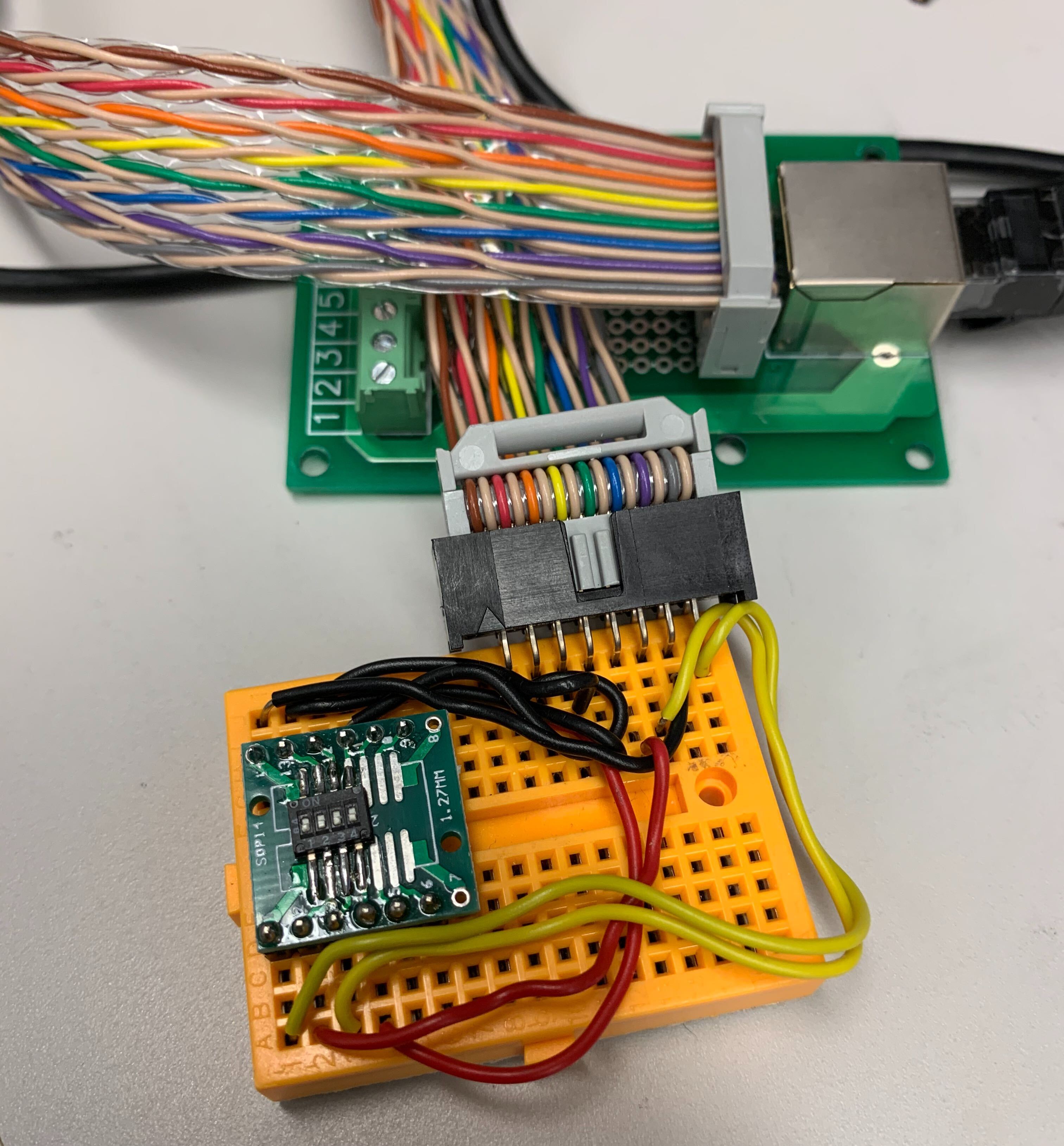
Connect JTAG programmer to
J17on the back of the board, bottom-center (the ribbon in the picture abvove). Connect blue jumpers betweenJ22(near ch8) pins 2 & 4 (V_pump) and betweenJ22pins 1 & 3 (V_jtag). You can zoom in the above picture (righ-click, view image) to check it. This configuration allows you to program the FPGA later on. -
Connect the raspberry Pi LVR monitor to the board, and activate the LVR monitor on the laptop if it is not already running. If not using the Pi, you can follow the instructions at the bottom of the page.
- Go to PuTTY and select Monitor Pi
- Both user name and password are "
lvr"
-
Set the power supply initially to 1.6V and the current limited to 2.0A, and connect provided input breakout board. Verify polarity of connections visually
- Red wire in positive terminal of power supply
- Blue wire in negative terminal
- Negative terminal ground shorted
- Turn power supply on and enable output
-
Adjust the
P1,P2, andP5potentiometers so that the 1.5V, 3.3V, and 5.5V rails (voltage plateaus) are set to those values.-
Slowly increase the input voltage from the initial 1.6V until either the 1.5V reading (
Vin_FPGA_1V5) stops increasing or exceeds 1.5V. At this point, tune the output using P1 to set it to 1.5V. You may have to increase the voltage more and iterate the tuning process. An alternate approach is given in the tip below. -
Resume raising the input voltage and repeat this process on the 3.3V (
Vin_FPGA_3V3) and 5.5V (V_OPAMP_RAIL) levels in the Pi LVR monitor. You should now be able to raise the input voltage all the way to 7V and the three readings should be stable.
Warning
STOP IF VALUES BELOW ARE EXCEEDED to prevent damage.
- 1.5V x 110% = 1.65V
- 3.3V x 110% = 3.63V
- The 5.5V rail (
Vop_rail) should not exceed 5.5V!!
When the power supply reaches about 4.5V, the expected input current given by the supply at this point should be around 0.09A. If it is substantially more there may be a problem
Tip
It may be useful to let the rail approach the desired value from below as input voltage increases, then turn down the rail plateau to a value below the desired final plateau, and make the final adjustments by turning the input voltage and rail plateau values up simultaneously. Note that you can verify the rail has reached its plateau if you increase the input voltage and the rail voltage no longer increases.
Desired values
- The 1.5V and 3.3V rails should be set to within 0.01V if possible.
- The 5.5V rail works in the 5.0-5.5V range, with a preference to be in the range 5.45-5.5V, as this allows for a slightly better time response.
-
-
Adjust the
P3andP4potentiometers to set utput standby configuration. Adjust the voltage offsets to 1.483V (1.2V LVR), 1.546V (1.5V LVR), or 1.775V (2.5V LVR) within a few mV at the following test point pairs using the following potentiometers, using a multimeter to read the DC voltage.- CH 4-1:
TP9(Vos_gen) andTP10(GND) - CH 8-5:
TP14(Vos_gen) andTP15(GND)
- CH 4-1:
-
Program the FPGA
- Initiate the program sequence, opening FlashPro on the laptop if is not already running
- If no program has been loaded onto the FPGA, go to Open Project and select the pre-loaded program in the LVR folder you want to run
- Go to Configure Device
- Click Browse, and select the file v2-06_lvr_fw.stp
- Set MODE to basic (should be default), and set ACTION to program
- Once that is complete, click PROGRAM
- Check in the log that the auto-verify ran successfully (
RUN PASSEDin green).
- Initiate the program sequence, opening FlashPro on the laptop if is not already running
-
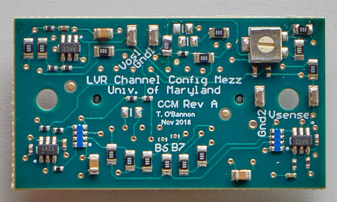
Turn off power and install all 8 CCMs in the orientation that allows you to read the silkscreen as shown below. Remove the Raspberry Pi connector to install those.
- For an
MStype LVR, set up master CCMs on odd channels, slaves on even. - For an
Atype LVR, place stand-alone single master (A) CCMs on all channels. - For
MSAtype, fill channels 1-4 withMSand 5-8 withACCMs.
- For an
-
Reduce power supply voltage to about 4.3V (1.2V LVR), 4.8V (1.5V LVR), or 5.3V (2.5V LVR) and check the under-voltage lockout (UVL) turns all channels off in the Rpi monitor.
- Set input voltage back to 7V
-
Change SW1 to
0011, and check the over-temperature protection turns all channels off and theLD7LED turns on. Some times you may have to go all the way to1111. -
Use the RJ45 breakout board to perform the sense line test. Verify that the voltage of a channel goes to RAIL when the corresponding sense lines are shorted to each other selecting the appropriate switches
Note
Slave channels will not alter voltage when shorting those channels. They will only go to RAIL when shorting their respective master channels.
-
SPI Communication test
- On the laptop's desktop, locate the "SPI test". Run this shortcut. The username and password are both 'spitest'
- Request WORD2, which should end with 0x206 (the FW version) and try modifying the config to turn all the channels OFF and ON again.
- Connect the SPI_RESET line (floating green wire) to any GND test point on the LVR and check that the response is all
00 00 00 00no matter the command you send until you allow the SPI_RESET to float once more.
-
Switch off the power and disconnect everything from the board (excluding the jumpers placed on
J22), and place colored stickers on the board near the CCM connectors to indicate which CCMs were used on the board during the QA. -
Make sure you update the database appropriately. You're done!
If not using the raspberry Pi LVR monitor
- Place a DVM (DC Voltage Meter) between
TP3(3.3V) andTP6(GND) to monitor the 3.3V rail - Add another DVM between
TP8(1.5V) andTP6(GND) to monitor the 1.5V rail - Add and a third DVM between
TP4(Vop_rail) andTP7(GND) to monitor the op amp rail.
The image below shows the location of TP3, TP6, and TP8, as well as potentiometers P1 and P2 that will be used to adjust the 1.5V and 3.3V rails.:
The image shows the locations of TP4, TP7, and P5 for the op amp rail.